Silicon Lenses Market Size
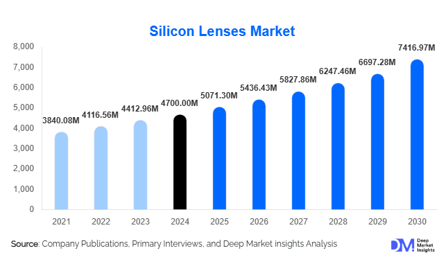
According to Deep Market Insights, the global silicon lenses market size was valued at USD 4,700 million in 2025 and is projected to grow from USD 5,071.3 million in 2026 to reach USD 7,416.97 million by 2031, expanding at a CAGR of 7.2% during the forecast period (2026–2031). The growth of the silicon lenses market is primarily driven by the rising adoption of infrared imaging systems, increasing deployment of LiDAR and ADAS technologies in automotive applications, and the integration of silicon lenses with wafer-level photonics for miniaturized and high-performance optical solutions.
Key Market Insights
- Infrared and thermal imaging applications dominate the market, driven by defense, security, and industrial inspection demands requiring high-transmission IR optics.
- Automotive adoption of LiDAR for autonomous vehicles is rapidly increasing, generating strong demand for compact and precise silicon lenses for ADAS modules.
- Asia-Pacific leads the market, with China, Japan, and South Korea driving demand due to manufacturing capabilities, LiDAR adoption, and expanding photonics infrastructure.
- North America remains a key market, led by U.S. defense, industrial, and automotive applications for high-performance IR optics.
- Technological integration, including wafer-level optics, MEMS-based fabrication, and photonics integration, is reshaping lens manufacturing efficiency and cost-effectiveness.
- Export-driven demand is significant, especially from China to North America and Europe for automotive and thermal imaging applications.
Silicon Lenses Market Trends
Miniaturization and Wafer-Level Optics
Manufacturers are increasingly adopting wafer-level optics and MEMS-based processes to produce compact, high-precision silicon lenses. These approaches reduce per-unit costs and improve alignment accuracy for integrated optical systems. Miniaturized lenses are enabling new applications in LiDAR, photonics, and portable IR devices. The trend is particularly significant in automotive and consumer electronics, where space-constrained optical modules require precise and reliable micro-lenses. Wafer-level fabrication also allows high-volume production, making high-performance silicon lenses more accessible to a broader set of industries.
Integration with Silicon Photonics
Silicon lenses are increasingly being integrated directly into silicon photonics platforms. This integration reduces packaging complexity, enhances optical alignment, and supports advanced telecom, data center, and optical computing applications. Companies are developing lenses optimized for wafer-level photonics, enabling the production of smaller, more efficient, and cost-effective optical modules. This trend accelerates adoption in high-tech industries and provides opportunities for new entrants with expertise in micro-optics and MEMS.
Silicon Lenses Market Drivers
Growth in LiDAR and Automotive Sensing
The increasing adoption of LiDAR sensors in autonomous and semi-autonomous vehicles is a major driver of silicon lenses demand. Automotive OEMs require precise, compact optics to ensure accurate sensing for ADAS and autonomous navigation. This has led to higher investment in wafer-level optics, MEMS fabrication, and large-scale lens production, pushing overall market growth. Rising commitments to vehicle automation across Europe, North America, and Asia-Pacific further accelerate this trend.
Rising Demand for Infrared Imaging Applications
Infrared and thermal imaging technologies in defense, security, healthcare, and industrial inspection are driving the market. Silicon lenses’ high IR transmission and durability make them essential for thermal cameras, spectrometers, and night-vision devices. The global emphasis on security infrastructure, industrial automation, and predictive maintenance is contributing to consistent demand growth.
Cost-Effective Manufacturing via Precision Molding
Advancements in precision molding and diamond-turning processes have improved yield and reduced production costs for silicon lenses. These methods allow large-scale manufacturing of standardized designs such as plano-convex lenses, which are widely used across multiple industries. The scalability of these processes supports adoption in high-volume applications like automotive LiDAR and consumer electronics, further fueling market expansion.
Silicon Lenses Market Restraints
High Manufacturing Costs
Precision silicon lens production requires specialized techniques, including diamond turning, deep reactive-ion etching, and wafer-level lithography. High capital investment and skilled labor requirements increase per-unit costs, limiting adoption in cost-sensitive applications. Smaller manufacturers may face barriers to entry, and price pressures can constrain growth in emerging markets.
Material Fragility and Yield Loss
Silicon is brittle, and defects in wafers can lead to yield losses during lens fabrication. Fragility complicates handling, assembly, and shipping, adding cost and limiting scalability. Manufacturers must implement strict quality control measures, which increases operational complexity and impacts overall profit margins.
Silicon Lenses Market Opportunities
Expansion of Automotive LiDAR Applications
LiDAR adoption for autonomous vehicles presents a rapidly growing opportunity. Silicon lenses provide the compact, high-precision optics required for these sensors. Market participants can leverage partnerships with automotive OEMs and LiDAR module producers to scale production, develop customized lens designs, and enter high-growth automotive supply chains.
Infrared Imaging in Security and Industrial Applications
Rising demand for thermal imaging and IR-based inspection creates opportunities in defense, industrial maintenance, and surveillance systems. Manufacturers can target government contracts, industrial automation projects, and security solutions. Offering lenses compatible with portable, high-resolution IR devices can open new customer segments.
Integration with Silicon Photonics
Silicon lenses can be integrated directly into photonic chips for telecommunications, optical computing, and quantum technologies. This reduces alignment issues and system complexity while supporting the trend toward compact and energy-efficient modules. Manufacturers focusing on wafer-level integration and photonics-compatible designs can capture significant growth in high-tech applications.
Report Scope
| Report Metric | Details |
|---|---|
| Market Size in 2025 | USD 4700 Million |
| Market Size in 2026 | USD 5071.3 Million |
| Market Size in 2031 | USD 7416.97 Million |
| CAGR | 7.2% (2026-2031) |
| Base Year for Estimation | 2025 |
| Historical Data | 2022-2024 |
| Forecast Period | 2026-2031 |
| Report Coverage | Revenue Forecast, Competitive Landscape, Supply Chain Disruption, Growth Factors, Environment & Regulatory Landscape and Trends |
| Geographies Covered | North America, Europe, APAC, Middle East and Africa, LATAM |
| Countries Covered | U.S., Canada, U.K., Germany, France, Spain, Italy, Russia, Nordic, Benelux, Rest of Europe, China, Korea, Japan, India, Australia, Singapore, Taiwan, South East Asia, Rest of Asia-Pacific, UAE, Turky, Saudi Arabia, South Africa, Egypt, Nigeria, Rest of MEA, Brazil, Mexico, Argentina, Chile, Colombia, Rest of LATAM |
Explore more data points, trends and opportunities Download Free Sample Report
Product Type Insights
Plano-convex lenses dominate the market, accounting for approximately 40–45% of 2025 revenues (USD 100–115 million). They are preferred for IR imaging, collimation, and general-purpose optical systems due to low-aberration performance and cost-effective fabrication. Meniscus and aspheric lenses are gaining traction in high-precision applications such as LiDAR and photonics modules, reflecting a trend toward customized optical solutions. The widespread adoption of plano-convex designs supports their continued leadership in the market.
Application Insights
Infrared imaging remains the largest application (35–40% market share, USD 85–100 million in 2025), driven by thermal cameras, spectrometers, and night-vision systems. LiDAR and sensing for automotive applications are growing rapidly, supported by autonomous vehicle development. Emerging applications include optical communications, quantum photonics, and portable spectroscopy, reflecting diversification into high-tech optical systems. Defense, industrial inspection, and consumer electronics also contribute significantly to market demand.
Distribution Channel Insights
Direct sales to OEMs, defense contractors, and photonics integrators dominate the distribution model. Some manufacturers supply through specialized optics distributors, particularly for research and smaller industrial applications. Strategic partnerships with automotive and photonics companies are increasingly important for high-volume, integrated lens solutions. Online B2B platforms are emerging for standardized lens designs, particularly in research and educational applications.
End-Use Industry Insights
Automotive, defense, and industrial applications are the leading end-use segments. Automotive LiDAR is the fastest-growing segment, with adoption driven by ADAS and autonomous vehicle requirements. Defense and security rely heavily on IR imaging and thermal systems. Industrial inspection and predictive maintenance also contribute significantly, as do emerging photonics-based applications in telecom and quantum computing. New entrants can explore niche applications such as environmental sensing and biomedical spectroscopy.
Explore more data points, trends and opportunities Download Free Sample Report
Silicon Lenses Market Segmentations
By Product Type
- Plano-Convex Lenses
- Plano-Concave Lenses
- Double-Convex (Bi-Convex) Lenses
- Double-Concave (Bi-Concave) Lenses
- Meniscus Lenses
- Aspheric / Customized Lenses
By Manufacturing / Fabrication Process
- Diamond Turning
- Precision Glass Molding
- Deep Reactive-Ion Etching (DRIE)
- Lithographic Fabrication (MEMS-based)
- Other Micro-Optic Methods
By Application
- Infrared Imaging / Thermal Cameras
- LiDAR & Sensing
- Spectroscopy
- Telecommunications / Optical Systems
- Defense / Aerospace
- Consumer Electronics
By End-Use Industry
- Automotive (ADAS / LiDAR)
- Healthcare / Medical Devices
- Consumer Electronics
- Industrial (Inspection / Monitoring)
- Aerospace & Defense
By Distribution Channel
- Direct OEM Sales
- Specialized Optics Distributors
- Online B2B Platforms
- Research & Educational Institutions
Regional Insights
North America
North America accounts for 25–30% of the market (USD 60–75 million in 2025), driven by the U.S. demand for defense, automotive, and industrial IR systems. Adoption of wafer-level optics and MEMS-based lenses is high, and OEMs prefer locally certified high-performance components. Canada contributes moderately through industrial and research applications.
Europe
Europe (20% market share, USD 50 million) shows strong growth in Germany, the U.K., and France. Automotive LiDAR adoption and industrial IR applications are key drivers. The region emphasizes sustainability, high-quality optical standards, and integration with European photonics initiatives.
Asia-Pacific
APAC (30–35% market share, USD 75–90 million) is the fastest-growing region, led by China, Japan, and South Korea. China’s large-scale manufacturing, LiDAR adoption, and export-oriented production are major drivers. Japan and South Korea focus on high-precision optics for industrial and photonics applications. India shows early-stage growth in the automotive and industrial sectors.
Latin America
Latin America contributes 5–8% (USD 12–20 million), with Brazil and Mexico showing modest adoption in automotive and industrial IR applications. Demand is limited by price sensitivity and lower domestic production capability.
Middle East & Africa
MEA also accounts for 5–8% (USD 12–20 million), driven by security, defense, and industrial monitoring applications. GCC countries (UAE, Saudi Arabia) and South Africa are primary contributors. Intra-African adoption of IR systems is emerging, though volume remains low.