Semiconductor Manufacturing Equipment Market Size
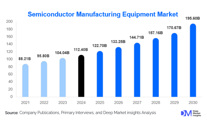
According to Deep Market Insights, the global semiconductor manufacturing equipment market size was valued at USD 112.4 billion in 2025 and is projected to grow from USD 122.7 billion in 2026 to reach USD 195.6 billion by 2031, expanding at a CAGR of 8.6% during the forecast period (2026–2031). The semiconductor equipment market growth is primarily driven by increasing demand for advanced chips powering artificial intelligence (AI), 5G infrastructure, electric vehicles (EVs), and data centers, along with significant government incentives for domestic chip manufacturing across North America, Europe, and Asia-Pacific.
Key Market Insights
- Rising global chip demand for AI, IoT, and autonomous systems continues to accelerate capital expenditure in wafer fabrication facilities (fabs).
- Government-backed semiconductor initiatives such as the U.S. CHIPS and Science Act, the EU Chips Act, and China’s “Made in China 2025” policy are fueling equipment investments.
- Foundry and logic segments dominate market share, driven by leading-edge process nodes (3nm and below) from TSMC, Samsung, and Intel.
- Asia-Pacific remains the largest regional market, supported by massive fab expansion in Taiwan, South Korea, Japan, and China.
- Advanced lithography and process control equipment are the fastest-growing categories, led by EUV technology adoption.
- Sustainability and energy efficiency in fabs are emerging as key investment priorities to reduce carbon footprint and water consumption.
Latest Market Trends
AI and High-Performance Computing (HPC) Driving Next-Gen Chip Production
The surge in artificial intelligence and machine learning workloads is propelling demand for advanced semiconductor equipment capable of producing high-density, high-efficiency chips. Leading manufacturers are scaling up investments in EUV lithography systems and advanced etching and deposition tools to meet AI chip design complexity. This trend is especially evident among foundries catering to NVIDIA, AMD, and emerging AI accelerator startups. The integration of chiplets and 3D packaging is also increasing demand for specialized bonding and metrology equipment.
Transition Toward Sustainable Semiconductor Manufacturing
Environmental sustainability is becoming central to semiconductor manufacturing strategy. Equipment vendors and fabs are investing in low-emission process gases, energy-efficient plasma systems, and water recycling technologies. Several leading players are introducing carbon-neutral manufacturing roadmaps. For instance, ASML and Applied Materials have committed to net-zero emissions targets by 2040, reflecting an industry-wide shift toward eco-innovation and responsible production practices.
Semiconductor Equipment Market Drivers
Rising Capital Investments in Advanced Nodes
As semiconductor nodes shrink below 3nm, equipment complexity and capital intensity increase significantly. Foundries are investing heavily in EUV and next-generation deposition and metrology tools to maintain competitive yield performance. The expansion of advanced fabs by TSMC, Samsung, and Intel is driving robust demand for lithography, etching, and wafer cleaning equipment. Continuous innovation in materials engineering and atomic-layer deposition is enabling further scaling and device performance improvements.
Global Push for Chip Independence
Geopolitical tensions and supply chain vulnerabilities exposed during the pandemic have triggered global efforts to establish local semiconductor ecosystems. The U.S., Europe, Japan, and India have announced multi-billion-dollar subsidy programs to attract fab construction and equipment manufacturing. These policies are directly boosting the procurement of semiconductor manufacturing tools, especially front-end wafer processing and testing equipment, across newly established fabs in the U.S. and Europe.
Market Restraints
High Cost and Complexity of Advanced Equipment
The capital intensity of semiconductor manufacturing continues to rise, with a single EUV lithography machine costing over USD 200 million. This creates significant barriers to entry for new market participants and limits equipment adoption to large-scale fabs. The steep cost of maintenance, complex installation processes, and long lead times also challenge production scalability and flexibility.
Geopolitical Risks and Export Restrictions
Trade tensions and export control policies, particularly between the U.S. and China, are restricting access to advanced semiconductor tools. U.S. restrictions on the export of EUV and DUV lithography systems to Chinese fabs have reshaped global supply dynamics. These geopolitical uncertainties create volatility in demand cycles and limit revenue opportunities for key suppliers.
Semiconductor Equipment Market Opportunities
Expansion in Power and Automotive Semiconductors
The electrification of vehicles and the growth of renewable energy infrastructure are fueling demand for power semiconductors such as SiC and GaN devices. Equipment manufacturers are capitalizing on this trend by developing specialized tools for wide-bandgap materials. Automotive chipmakers are expanding capacity for ADAS and EV powertrain components, opening new opportunities for mid-tier equipment suppliers focused on deposition, testing, and packaging technologies.
Emergence of 3D ICs and Advanced Packaging
With Moore’s Law slowing, semiconductor firms are shifting focus to 3D integration and heterogeneous packaging. This creates demand for new classes of bonding, inspection, and metrology tools. Equipment innovations enabling chip stacking, wafer-level packaging, and high-density interconnects are becoming critical to meet performance and power efficiency requirements for AI and mobile applications.
Report Scope
| Report Metric | Details |
|---|---|
| Market Size in 2025 | USD 112.4 Billion |
| Market Size in 2026 | USD 122.7 Billion |
| Market Size in 2031 | USD 195.6 Billion |
| CAGR | 8.6% (2026-2031) |
| Base Year for Estimation | 2025 |
| Historical Data | 2022-2024 |
| Forecast Period | 2026-2031 |
| Report Coverage | Revenue Forecast, Competitive Landscape, Supply Chain Disruption, Growth Factors, Environment & Regulatory Landscape and Trends |
| Geographies Covered | North America, Europe, APAC, Middle East and Africa, LATAM |
| Countries Covered | U.S., Canada, U.K., Germany, France, Spain, Italy, Russia, Nordic, Benelux, Rest of Europe, China, Korea, Japan, India, Australia, Singapore, Taiwan, South East Asia, Rest of Asia-Pacific, UAE, Turky, Saudi Arabia, South Africa, Egypt, Nigeria, Rest of MEA, Brazil, Mexico, Argentina, Chile, Colombia, Rest of LATAM |
Explore more data points, trends and opportunities Download Free Sample Report
Product Type Insights
Front-end equipmentincluding lithography, etching, deposition, and cleaning systemsaccounts for the largest share of the market, driven by continuous process node advancements. Back-end equipment for assembly, testing, and packaging is growing steadily due to increasing adoption of 3D packaging and system-in-package (SiP) solutions. Among these, lithography equipment remains the highest revenue contributor, dominated by EUV systems from ASML, followed by deposition and metrology tools from Applied Materials and KLA Corporation.
Application Insights
Foundry and logic segments dominate, supported by strong demand from fabless semiconductor companies producing AI, HPC, and mobile processors. Memory manufacturingincluding DRAM and NANDremains a key application area, especially as hyperscale data centers expand. Analog and power device production is also gaining traction, driven by EV adoption, renewable energy systems, and industrial automation.
Explore more data points, trends and opportunities Download Free Sample Report
Semiconductor Manufacturing Equipment Market Segmentations
By Product Type
- Front-End Equipment (Lithography, Etching, Deposition, Cleaning)
- Back-End Equipment (Assembly, Packaging, Testing)
- Metrology and Inspection Equipment
- Others (Automation, Material Handling, and Support Systems)
By Application
- Foundry and Logic
- Memory (DRAM, NAND)
- Analog and Power Devices
- Discrete and Sensor Devices
Regional Insights
Asia-Pacific
Asia-Pacific remains the global hub for semiconductor equipment consumption, led by Taiwan, South Korea, Japan, and China. TSMC, Samsung, and SK Hynix continue to dominate investment in advanced fabs. China’s ongoing push for semiconductor self-sufficiency underpins robust domestic demand, even amid U.S. export restrictions. Japan remains a critical supplier of materials and precision equipment components.
North America
North America’s semiconductor equipment market is expanding rapidly, driven by large-scale fab construction projects supported by the U.S. CHIPS and Science Act. Intel, TSMC, and Samsung are investing in new facilities in Arizona, Texas, and Ohio. Domestic equipment suppliers such as Applied Materials, Lam Research, and KLA are benefiting from reshoring and localization trends.
Europe
Europe is experiencing a revival in semiconductor manufacturing, supported by the EU Chips Act and major investments by companies such as STMicroelectronics, Infineon, and GlobalFoundries. Germany, France, and the Netherlands are leading equipment demand, with strong emphasis on automotive and industrial semiconductors.
Japan
Japan remains a key market and supplier base for semiconductor manufacturing equipment, particularly in deposition, cleaning, and inspection technologies. Companies such as Tokyo Electron, Nikon, and Canon play central roles in supporting both domestic and international fabs with precision tools and process expertise.
Key Players in the Semiconductor Manufacturing Equipment Market
- ASML Holding N.V.
- Applied Materials, Inc.
- Lam Research Corporation
- Tokyo Electron Limited
- KLA Corporation
- Nikon Corporation
- Canon Inc.
- Screen Semiconductor Solutions Co., Ltd.
- Advantest Corporation
- ASM International N.V.